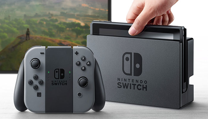
The much awaited Nintendo Switch was released recently and fans couldn’t wait to get their hands on the latest console-table hybrid. With great graphics, loads of game titles and incredible performance, Nintendo Switch is really fun to play. Nvidia had shared the information on what it takes to develop a gaming console like Nintendo Switch – serious engineering! The development, Nvidia claims, encompassed 500 man-years of effort across every facet of creating a new gaming platform, right from complicated algorithms, system design to APIs and game engines.

Nintendo Switch teardown reveals stock Nvidia Tegra CPU and Maxwell GPU
Nvidia had already revealed that Nintendo Switch is powered by the performance of the custom Tegra processor. According to Nvidia, “The high-efficiency scalable processor includes a NVIDIA GPU based on the same architecture as the world’s top-performing GeForce gaming graphics cards. The Nintendo Switch’s gaming experience is also supported by fully custom software, including a revamped physics engine, new libraries, advanced game tools and libraries.” Based on Nvidia’s announcement, it was speculated that Nintendo Switch would come with Nvidia Pascal Parker architecture. Other reports claimed that it would be based on Maxwell.

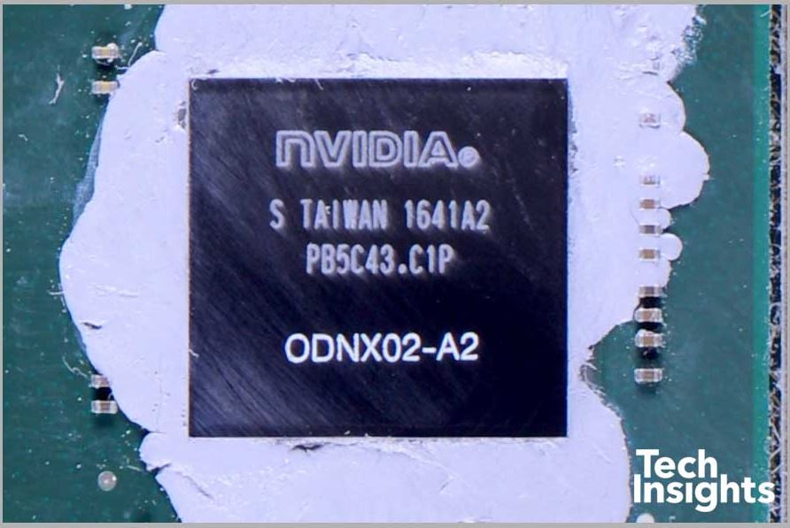
The exact nature of the architecture had remained unknown until Tech Insights did a teardown of Nintendo Switch. Nintendo Switch, as the teardown shows, uses a stock Tegra X1 processor which hasn’t been customized at all. So what Nvidia claimed as “custom” Tegra processor is after all the stock Tegra X1! “After subsequent processing of the GPU from the Nintendo Switch, we have determined that the processor is the NVIDIA Tegra T210. The T210 CPU features 4 Cortex A57 and 4 Cortex A53 processor cores and the GPU is a GM20B Maxell core”, says the report. The teardown also talks about several interesting features of the Nintendo Switch hardware, including a docking station, joy-con controllers, joy-con IR camera module, mystery of the joy-con connectivity and more!
