Nvidia’s highly anticipated Pascal GeForce GTX 1080 and GTX 1070 graphics cards are launching this summer sweclockers.com has confirmed. While the more budget friendly GTX 1060 that’s positioned to give gamers a lot of bang for their buck is scheduled to debut this fall, the Swedish pub revealed.
The GeForce GTX 1080 and GTX 1070 graphics cards are based on Nvidia’s upcoming Pascal GP104 GPU. Measuring roughly 300mm² according to a leaked photo, GP104 is set to replace Nvidia’s current mid range Maxwell GTX 900 series offerings in Nvidia’s current product stack. Which includes the GM204 powered GeForce GTX 980 and GeForce GTX 970 graphics cards.
Nvidia’s Pascal GeForce GTX 1080, GTX 1070 And GTX 1060 Graphics Cards – Faster & More Affordable
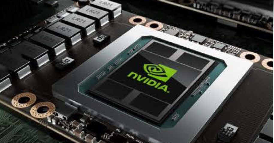
If Nvidia’s recently announced Tesla P100 is anything to go by then the upcoming gaming oriented Pascal graphics cards replacements are poised to deliver significant performance gains and power efficiency gains. Even compared to the company’s flagship GTX 980 Ti and Titan X graphics cards. Earlier last week, news broke of Nvidia allegedly discontinuing its GTX 980 Ti, GTX 980 and GTX 970 graphics cards in preparation for Pascal’s launch this June.
Credit : Videocardz.com
The GTX 1060 – which is actually merely placeholder name until we figure out what Nvidia plans to call its new GTX series, is based on the company’s GP106 GPU. Which measures less than 200mm², coming in at roughly one third the size of the monstrous GP100 GPU that was demonstrated at GTC earlier this month.
The graphics chip is purported to be quite frugal when it comes to power consumption as the GTX 1060 is said to not require any PCIe power connectors and can simply run off the 75W provided by the PCIe slot in a similar fashion to Nvidia’s GTX 750 Ti. So we’re potentially looking at the new “console killer” here.
| GTX 980 Ti | GTX 980 | GTX 1080 | GTX 1070 | GTX 1060 | TESLA P100 (GP100) | |
| GPU | GM200 | GM204 | GP104 | GP104 | GP106 | GP100 |
| Process Node | 28nm | 28nm | 16nm FinFET | 16nm FinFET | 16nm FinFET | 16nm FinFET |
| Transistors | 8 Billion | 5.2 Billion | TBA | TBA | TBA | 15.3 Billion |
| CUDA Cores | 2816 CUDA Cores | 2048 CUDA Cores | ~2560 CUDA Cores | ~2048 CUDA Cores | ~1280 CUDA Cores | 3840 CUDA Cores |
| VRAM | 6 GB GDDR5 | 4 GB GDDR5 | 8 GB GDDR5X | 8 GB GDDR5 | 4 GB GDDR5 | 16GB HBM2 |
| Memory Bus | 384-bit | 256-bit | 256-bit | 256-bit | 128-bit | 4096-bit |
| Memory Speed | 7Gbps | 7Gbps | 10-12Gbps | 8Gbps | 8Gbps | 1.4Gbps |
| Bandwidth | 336GB/s | 224GB/s | 384-320GB/s | 256GB/s | 128GB/s | 720GB/s |
| TDP | 250W | 165W | TBA | TBA | TBA | 300W |
| Launch Date | May 2015 | September 2014 | June 2016 | June 2016 | Autumn 2016 | 2017 |
Nvidia’s Brand New Graphics Architecture – One Step Closer To 4K Gaming Nirvana
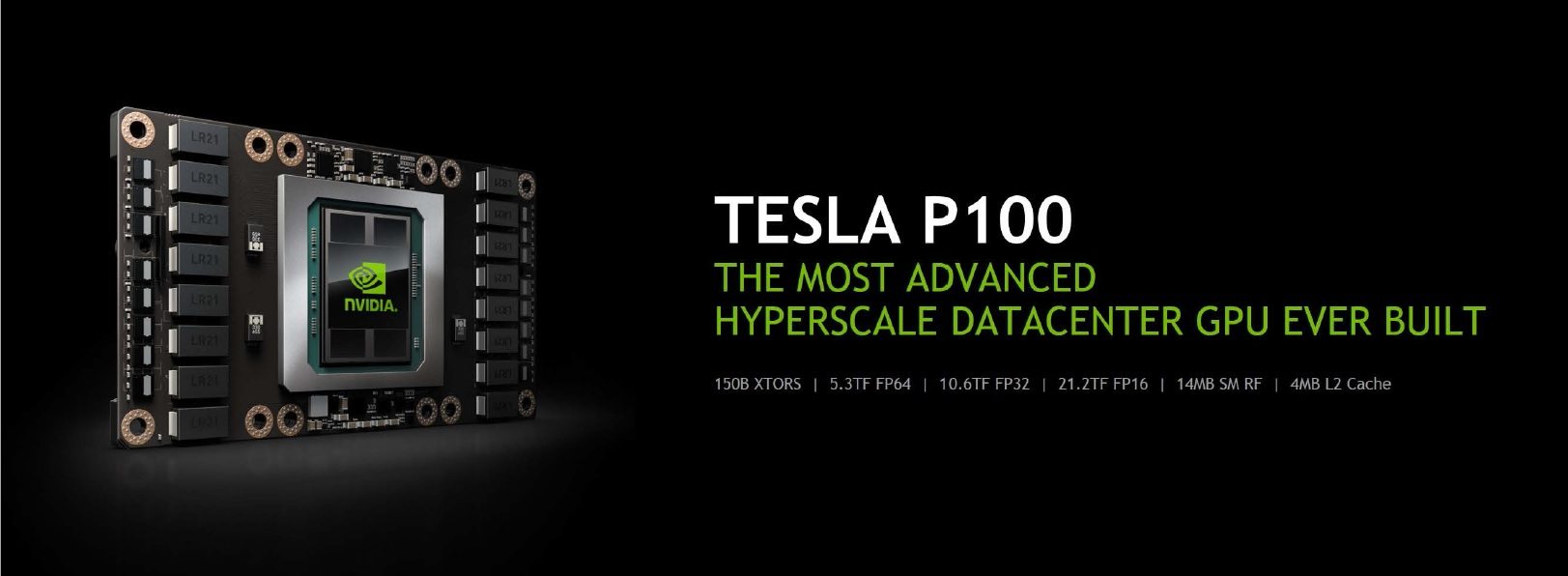
At his keynote earlier this month during GTC 2016 Jen-Husn Huang, Nvidia’s Co-Founder & CEO introduced the company’s very first Pascal graphics chip. The Tesla P100 accelerator, based on the largest ever GPU produced by the company code named GP100.
Jen-Hsun went on to distill down what he believed made Pascal great to four key ingredients and they are :
– Next generation Pascal graphics architecture.
– TSMC 6nm FinFET process technology.
– Second generation stacked High Bandwidth Memory.
– NV-Link GPU interconnect.

Nvidia is bringing a major architectural overhaul and several adjuvent advancements to deliver more gaming and compute performance at lower power and cost. The foundation of it all is TSMC’s 16nm FinFET process technology. Which enables tremendous power efficiency and frequency gains over current 28nm planar technology that’s deployed across Nvidia’s GeForce GTX 900 series and AMD’s Radeon 300 series.
Additionally Nvidia has made a number of very significant changes to the architecture with Pascal which the company has published in a whitepaper right after GTC. For starters the company is bringing back double precision floating point compute performance to the forefront. Where only one double precision CUDA core existed for every 32 standard CUDA cores in Maxwell, Pascal is built with one double precision CUDA core for every two standard CUDA cores. That’s sixteen times more than Maxwell and allows the company to compete again in the High Performance Computing fields where double precision rules supreme.
The New Pascal Building Block
The basic building block of every Pascal GPU is called the the streaming multiprocessor or SM for short. The streaming multiprocessor is a graphics and compute engine that schedules and executes instructions on many threads simultaneously.

Each Pascal streaming multiprocessor houses 64 FP32 CUDA cores, half that of a Maxwell SM. Within each Pascal streaming multiprocessor there are two 32 CUDA core partitions, two dispatch units and a brand new, smarter, scheduler. In addition to an instruction buffer that’s twice the size of Maxwell per CUDA core.This gives each Pascal CUDA core access to twice the registers vs Maxwell.
The end result is more performance per clock per CUDA core, lower power consumption and a higher overall clock speed. All of which were exemplified in the impressive Tesla P100 specs. The updated hardware scheduler also extends Pascal’s abilities to execute code asynchronously, which will no doubt have a positive impact on the architecture’s performance when it comes to DirectX 12 Async Compute.
| Tesla Products | Tesla K40 | Tesla M40 | Tesla P100 |
| GPU | GK110 (Kepler) | GM200 (Maxwell) | GP100 (Pascal) |
| SMs | 15 | 24 | 56 |
| TPCs | 15 | 24 | 28 |
| FP32 CUDA Cores / SM | 192 | 128 | 64 |
| FP32 CUDA Cores / GPU | 2880 | 3072 | 3584 |
| FP64 CUDA Cores / SM | 64 | 4 | 32 |
| FP64 CUDA Cores / GPU | 960 | 96 | 1792 |
| Base Clock | 745 MHz | 948 MHz | 1328 MHz |
| GPU Boost Clock | 810/875 MHz | 1114 MHz | 1480 MHz |
| Compute Performance - FP32 | 5.04 TFLOPS | 6.82 TFLOPS | 10.6 TFLOPS |
| Compute Performance - FP64 | 1.68 TFLOPS | 0.21 TFLOPS | 5.3 TFLOPS |
| Texture Units | 240 | 192 | 224 |
| Memory Interface | 384-bit GDDR5 | 384-bit GDDR5 | 4096-bit HBM2 |
| Memory Size | Up to 12 GB | Up to 24 GB | 16 GB |
| L2 Cache Size | 1536 KB | 3072 KB | 4096 KB |
| Register File Size / SM | 256 KB | 256 KB | 256 KB |
| Register File Size / GPU | 3840 KB | 6144 KB | 14336 KB |
| TDP | 235 Watts | 250 Watts | 300 Watts |
| Transistors | 7.1 billion | 8 billion | 15.3 billion |
| GPU Die Size | 551 mm² | 601 mm² | 610 mm² |
| Manufacturing Process | 28-nm | 28-nm | 16-nm |
The clock is ticking and we’re less than two months away from Computex where Nvidia is purported to debut its gaming Pascal graphics cards. It’s been over four years since the first 28nm GTX 600 series graphics cards were introduced and it looks like the next generation of GPUs on FinFET could very well have been worth the wait.


