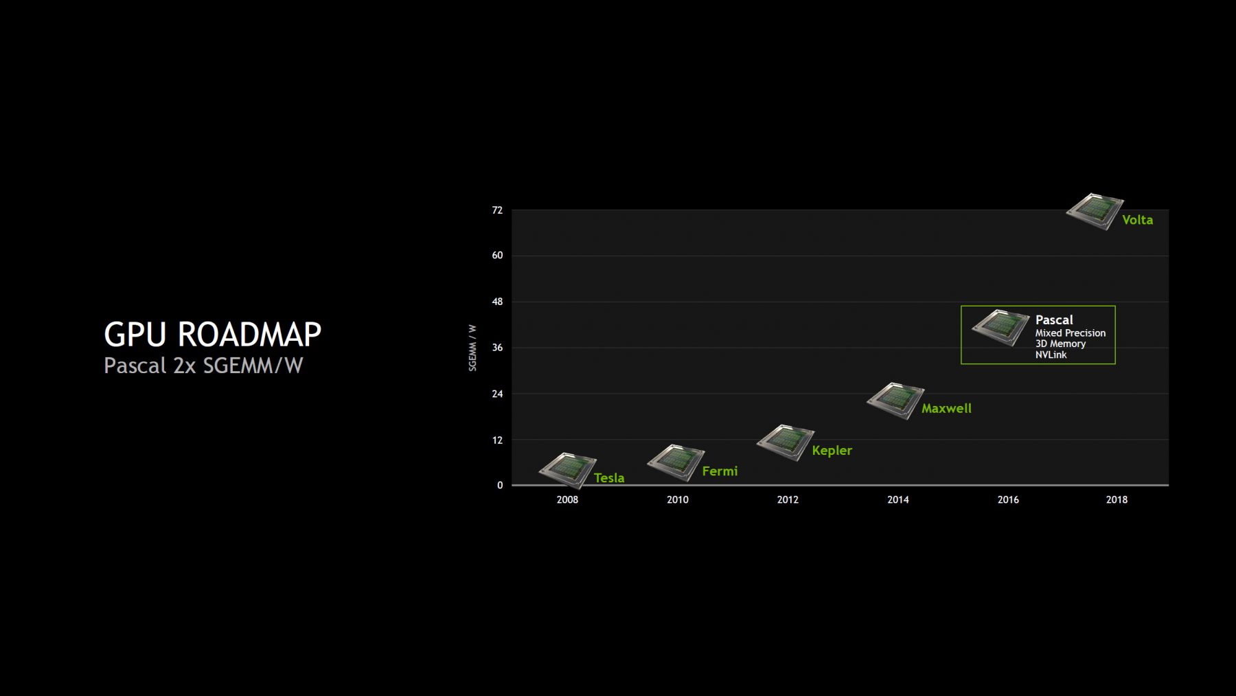
Nvidia had announced the Volta Next Generation GPU ages ago. The Volta GPU was expected to be Nvidia’s next gen chip architecture – a replacement for the now famous and widely used Maxwell architecture. But the Volta GPU launch was pushed to accommodate Pascal graphics card lineup. In the earnings call, Nvidia confirmed that they have taped out all Pascal GPUs. The development of Pascal architecture cost Nvidia about 3 billion dollars. Now that most of the products in Pascal lineup have been launched, Nvidia plans to concentrate on their latest GPU project.

GV102, GV104 and GV110 GPUs to feature Volta Architecture
As reported by Motley Fool, the Volta is expected to be a monster – with a large performance boost. Motley fool refers to the post on Baidu from user USG Ishimura and according to a translation of USG Ishimura’s post, the performance of GV104 – the Volta-based successor to the recently released GP104 chip – is expected to offer “really strong” performance. The site also mentions that development of 3 GPUs based on Volta architecture is in progress.

These three chips have been rumored to introduce high-end gaming GPUs –
- GV110 GPU
- GV102 GPU
- GV104 GPU
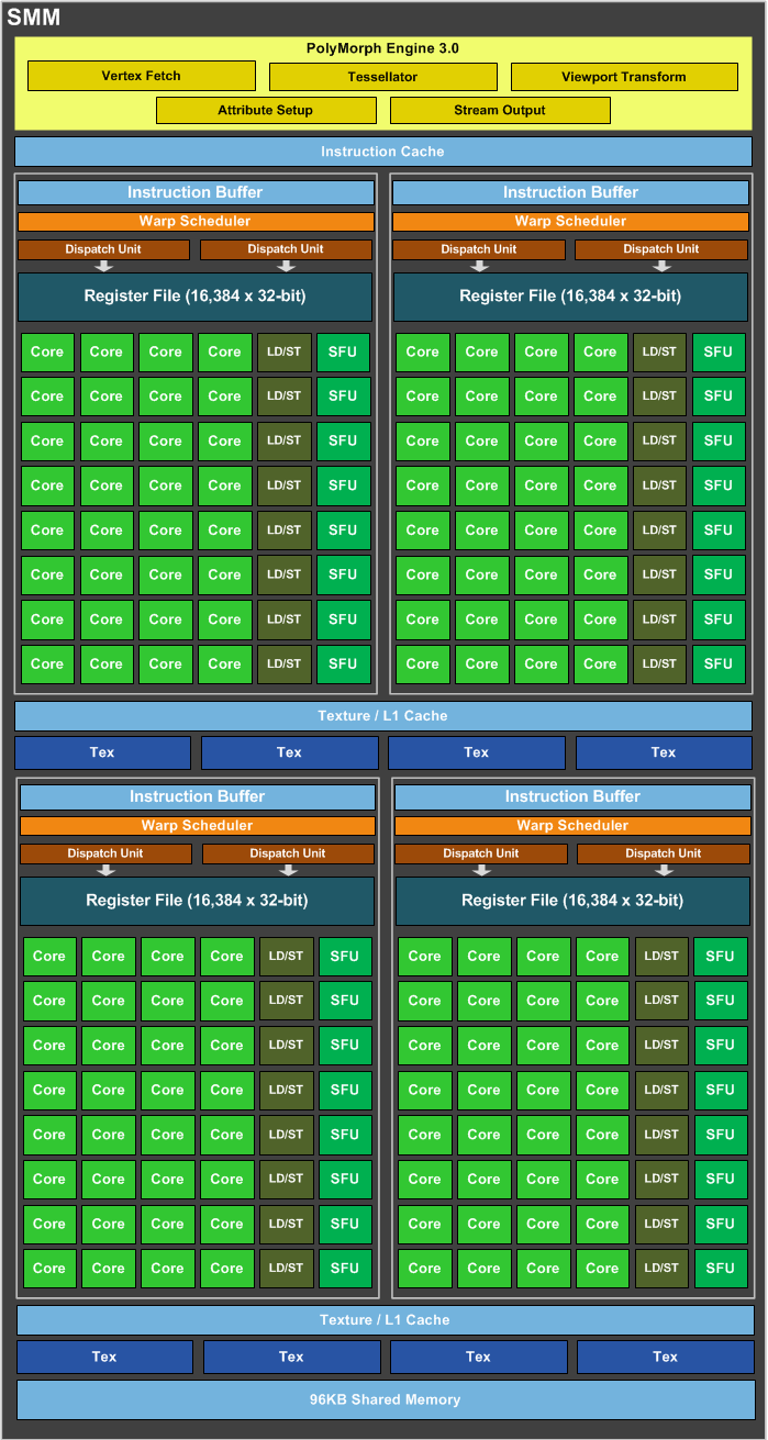
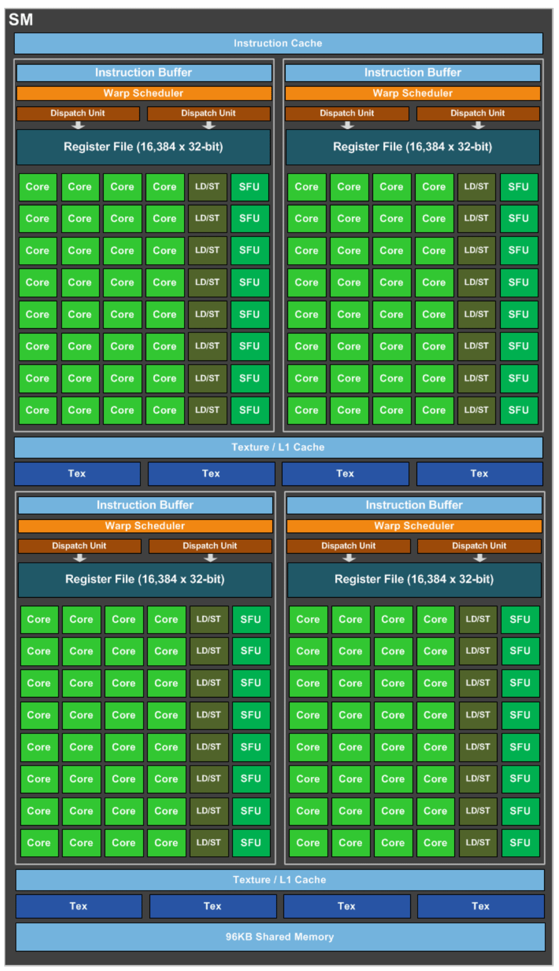
If rumors are to be believed, Volta architecture is completely different from Pascal. Nvidia has revamped and redesigned the architecture to give performance enhancements and boost to meet high-end gaming requirements. It’s worth noting that although Pascal architecture had significant performance benefits over Maxwell, both shared a common DNA. The SM designs for both is similar.
Maxwell GM204 and Pascal GP104 SM Designs


GV102, GV104 For High-End Gaming, But GV110 also for Consumer Market?
GV104 GPU will replace the GP104 GPU and will come with an affordable price tag. GV102 is the successor for GP102 (housed inside GeForce GTX Titan X card). This is aimed at gaming enthusiasts demanding super horsepower. GV110 is expected to be full fat chip with limited FP64 capabilities designed for consumer market, as reported by wccftech.
Below is a comparison of AMD Polaris, Vega, Nvidia Pascal and Volta specs –
| GPU Family | AMD Polaris | AMD Vega | NVIDIA Pascal | NVIDIA Volta |
| Flagship GPU | Polaris 10 | Vega 10 | NVIDIA GP100 | NVIDIA GV110 |
| GPU Process | GloFo 14nm FinFET | GloFo 14nm FinFET | TSMC 16nm FinFET | FinFET |
| GPU Transistors | TBC | 15-18 Billion | 15.3 Billion | TBD |
| Memory (Consumer Cards) | GDDR5 | GDDR5X/HBM2? | GDDR5X/HBM2? | HBM2 |
| Memory (Dual-Chip Professional/ HPC) | GDDR5 | HBM2 | HBM2 | HBM2 |
| HBM2 Bandwidth | 256 GB/s | 1 TB/s (Peak) | 1 TB/s (Peak) | 1 TB/s (Peak) |
| Graphics Architecture | GCN 4.0 (Polaris) | GCN 4.0 (Vega) | 5th Gen Pascal CUDA | 6th Gen Volta CUDA |
| Successor of (GPU) | Radeon 300 Series | Radeon Fury Series | GM200 (Maxwell) | GV110 (Volta) |
| Launch | 2016 | 2017 | 2016 | 2017-2018 |
Official announcement from Nvidia on Volta is expected in their GTC presentation scheduled for 2017. Meanwhile, expect to hear more about Pascal based GP102 and GP100 since they are yet to be introduced in the market.
