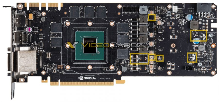
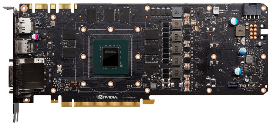
While the flagship Nvidia GeForce GTX 1080 is enjoying all the attention, fans are also eyeing the next-best graphics card, the GTX 1070. Specs and hardware details of the card have already been out for quite some days now, and we have also seen the GTX 1070 images that look exciting. After a lot of important leaks, today the Nvidia GTX 1070 PCB has leaked out in an image found by Videocardz.

The image above is of the PCB of the GTX 1070, and the yellow markers are meant to indicate the parts that are absent in this card but are present in the GTX 1080. As you can clearly notice from the images of the PCBs of the GTX 1080 vs GTX 1070, there’s just cosmetic difference between the two. Nvidia could have easily added water-blocks to the GTX 1070 along with one more VRM phase, but the company knows how to space its products properly for good business.

Here’s the surprising part. The GTX 1070 Founder’s Edition is blocked at 112% TDP currently for reasons unknown, and a limit has been placed on overclocking, keeping the card at a maximum of 1980-2050 MHz. It seems like Nvidia applied these limits deliberately to make sure that the GTX 1070 has all the potential to be a flagship graphics card but the GTX 1080 still takes the crown, purely for business purposes. The GTX 1070, unlike the flagship, can still draw more from the single 8-pin power connector. It is advised to wait for GP104-200 silicon-based custom cards.

Reports have already started coming in that the GTX 1070 is on par with the GTX 980Ti or even better in some areas. With a starting price of $379 for the regular version, the new Nvidia GeForce GTX 1070 is a good upgrade for those who are still on the GTX 970.
