
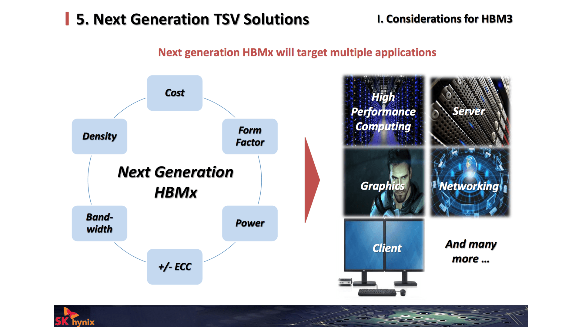
The first generation and second generation High Bandwidth Memory (HBM) have already made few appearances in shipping products. Samsung and Hynix are already working on the follow-up – the third generation of HBM, called HBM3. At the Hot Chips symposium in Cupertino, HBM3 is expected to offer improved density, bandwidth and power efficiency.
What differentiates HBM from conventional memory setups is the fact that while RAM chips are placed next to each other on a circuit board, HBM stacks a bunch of RAM dies on top of each other, connecting them directly using Through-Silicon Vias (TVS).
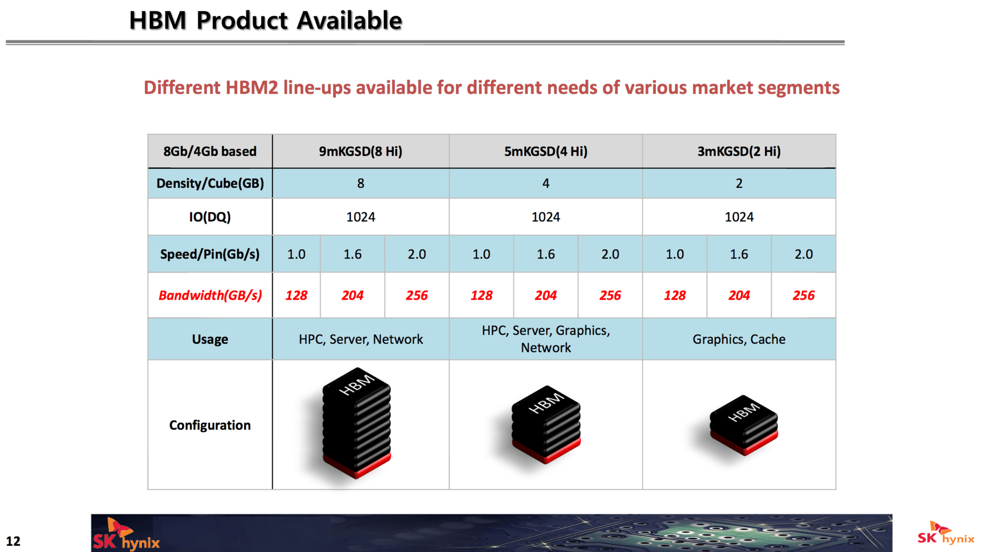
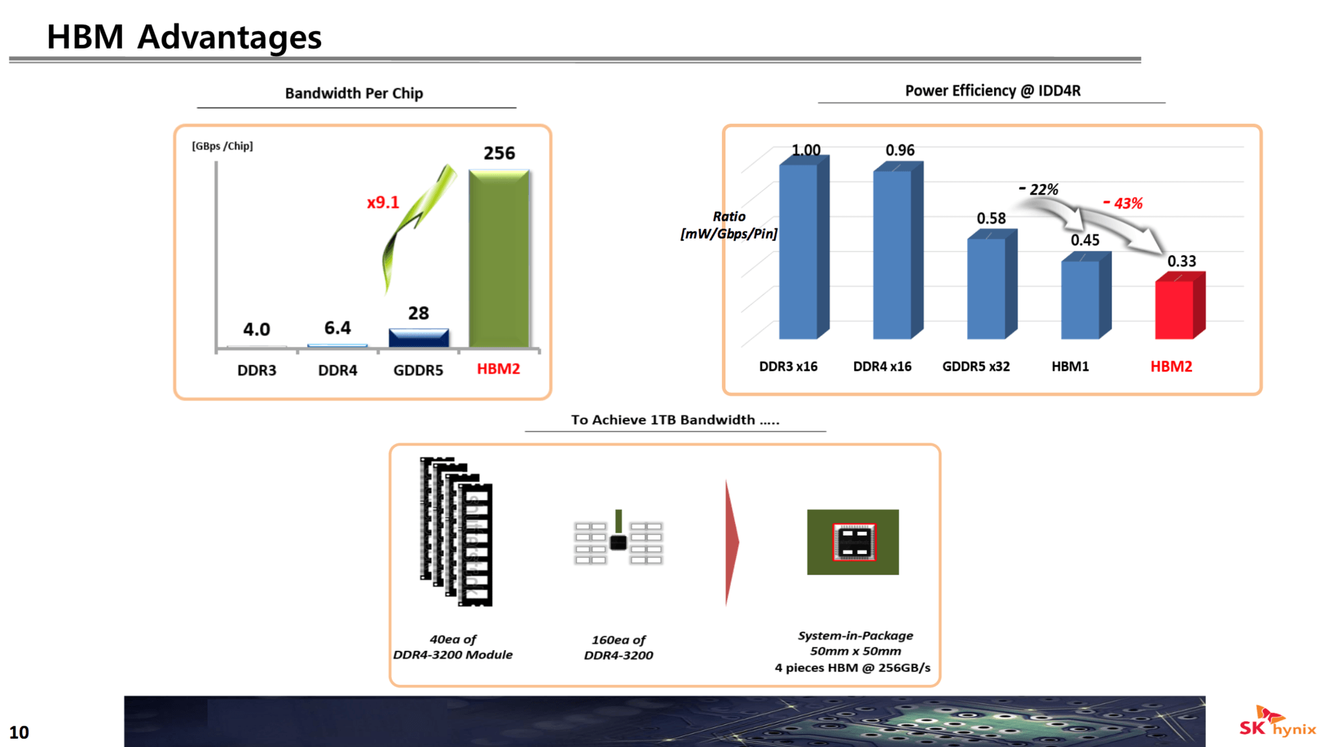
At the Symposium, SK Hynix clarified that the company is looking forward to expand HBM technology into 3 different markets: HPC&Servers, Network&Graphics, and Client-DT&Notebooks. HBM2 will offer capacities up to 32GB through 4 stacks of 8 Hi modules.
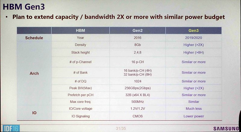
HBM3
Hynix is already working on HBM3. No specific details about the first graphics architecture to use HBM3 are known. It appears that AMD Navi is expected to support the next generation memory. It remains to be seen whether this memory is HBM3 or GDDR6.
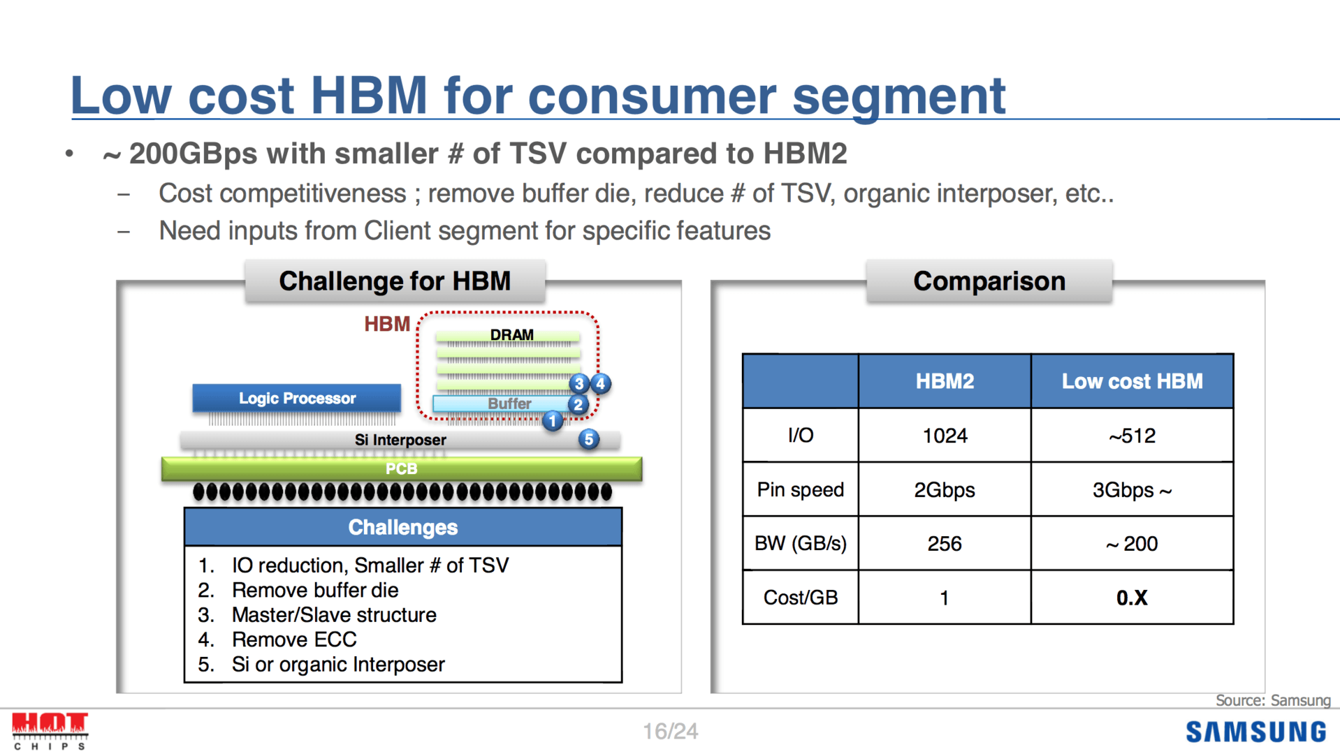
Samsung is also working on HBM3 and shared these details –
GDDR6
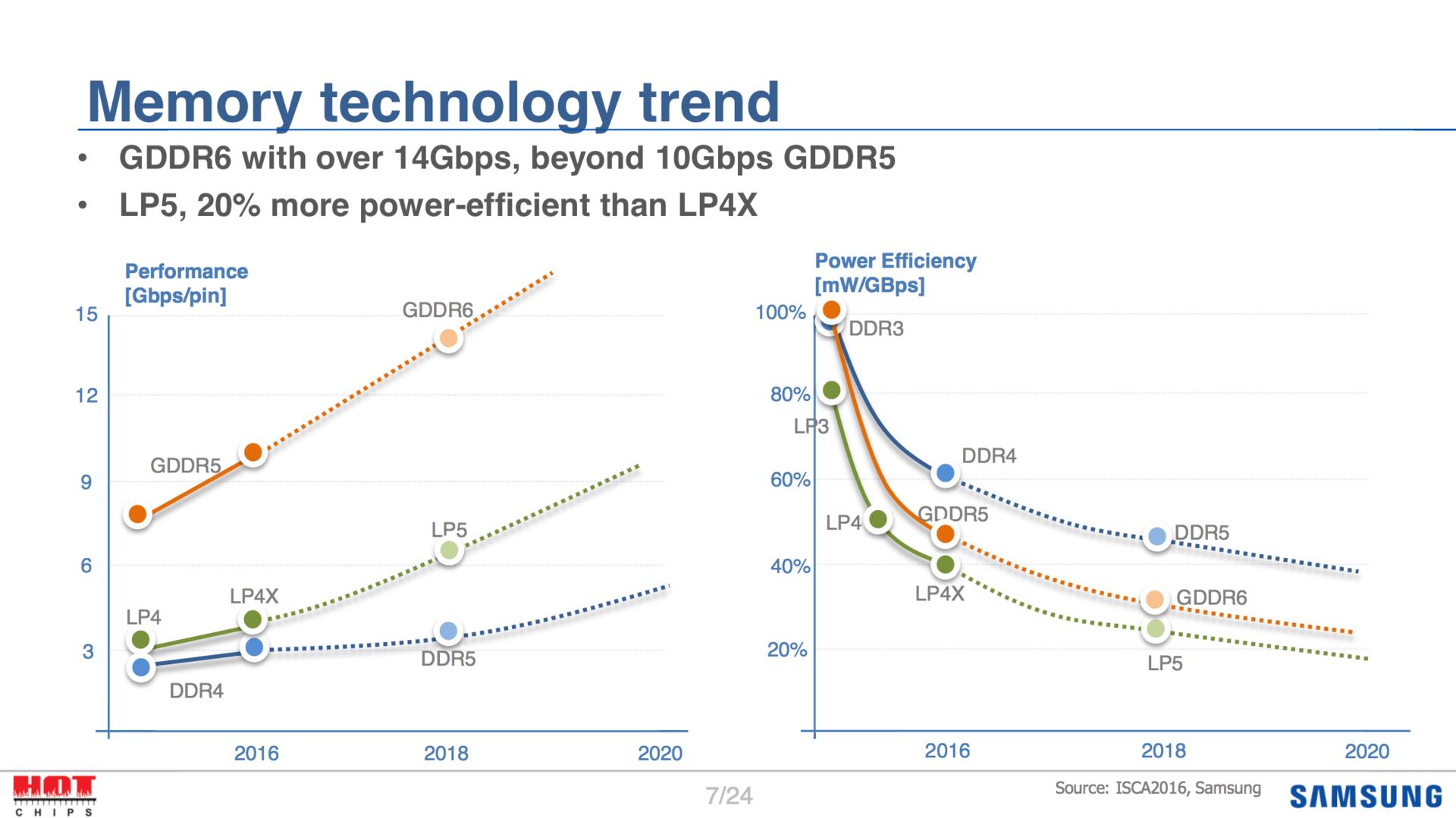
Samsung has announced the availability of Graphics Double Data Rate (GDDR) in 2018. GDDR6 is a type of Synchronous Dynamic Access Memory designed for a graphics processor. GDDR6 is expected to offer more than 14Gb per second of bandwidth, more than GDDR5X announced by Micron earlier this year.
Samsung revealed the roadmap of GDDR6 –
The HBM3 is very likely to be seen in AMD’s Navi graphics core architecture that’s slated for a 2019/2020 release. And the GDDR6 will make its appearance sometime in 2018.